


0.5mm BGA copper to hole clearance on inner layers
 View
View
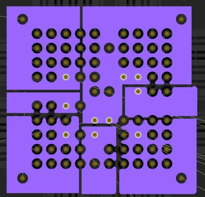
According to the BGA layout guidance, for 0.5mm pitch BGAs it is suggested to remove unused via pads on inner layers. https://jlcpcb.com/blog/bga-design-rules What is the minimum copper pour to drill-hole spacing for this on 6+ layer PCB with via-in-pad? And what is the minimum track to drill-hole spacing? Other pages state 0.2 mm but this wouldn't be compatible with routing on the inner layer as suggested in the BGA layout page. Example below with unused pads removed, and 0.12 mm hole to copper spacing in the photo.
PCB
Sign In Or Register Comment after
No comments yet. Be the first to comment!